

As the "nerve center" of electronic devices, the manufacturing level of PCBs (Printed Circuit Boards) directly affects device performance and stability. With the growing demand for "miniaturization, high integration, and long service life" in fields such as smartphones, automotive electronics, and industrial control, PCB Fabrication—with its precise processes and flexible adaptability—has become a key link supporting the development of the electronics industry. Its four core characteristics closely align with industry needs.
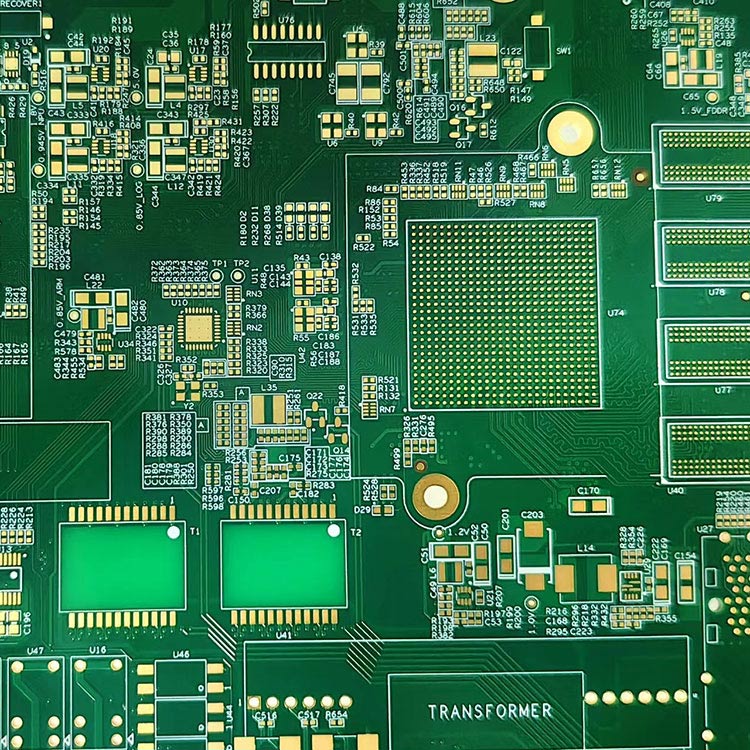
The miniaturization of electronic devices has driven the continuous reduction of PCB line widths and hole diameters, making high-precision manufacturing a core competitive advantage:
Laser Direct Imaging (LDI) technology is adopted, enabling line width and line spacing control within 0.05–0.1mm—only 1/3 of that achievable with traditional processes. This meets the "high-density wiring" needs of smartphones and wearable devices;
Drilling accuracy reaches ±0.01mm, allowing the processing of micro-blind holes smaller than 0.15mm. This enables more components to be integrated into the limited area of a PCB. For example, a smartwatch PCB can integrate multiple modules (communication, sensing, power supply, etc.), increasing functional density by 40% compared to traditional PCBs.
PCB Fabrication involves over 20 core processes, and full-process collaboration is key to quality assurance:
Each link—from substrate cutting and circuit etching to solder mask printing and finished product inspection—requires precise control. For example, the etching process uses an automated spray system, and the circuit etching uniformity error is ≤5%. This avoids device short circuits caused by uneven circuits;
The introduction of automatic optical inspection (AOI) technology has a detection coverage rate of up to 99.8%, which can quickly identify defects such as line gaps and pad offsets, and control the finished product defect rate to below 0.5%. It is suitable for scenarios with strict reliability requirements such as automotive electronics and medical equipment.
Electronic devices in different fields have significantly different requirements for PCB material properties, and manufacturers can flexibly adapt:
High-frequency communication equipment (e.g., 5G base stations) uses Rogers high-frequency substrates, with dielectric constant stability error ≤2%, reducing signal transmission loss by 30%;
Automotive electronics PCBs use high-temperature-resistant FR-4 substrates, which can withstand high-low temperature cycles of -40℃~125℃. This meets the needs of high-temperature environments such as engine compartments and charging piles, with a service life of over 10 years—twice that of ordinary PCBs.
Faced with stricter environmental policies, PCB Fabrication is speeding up the use of green processes:
Lead-free soldering processes are promoted, with lead content ≤1000ppm, and this meets the EU RoHS standard;
Wastewater recycling systems are set up, and the etching wastewater recovery rate reaches over 95%. Also, heavy metal emission concentrations are 50% lower than national limits. Also, recyclable substrates are used to reduce industrial solid waste, and this fits the "low-carbon manufacturing" trend of the electronics industry.
| Core Characteristics | Core Indicators | Adapted Scenarios | Key Value |
|---|---|---|---|
| High-Precision Manufacturing | Line width: 0.05–0.1mm; Drilling accuracy: ±0.01mm | Smartphones, wearable devices | High-density integration, reducing device size |
| Multi-Process Collaboration | AOI detection rate: 99.8%; Defect rate: ≤0.5% | Automotive electronics, medical equipment | Strict quality control, improving device reliability |
| Flexible Material Adaptation | High-frequency substrate dielectric loss: ≤0.002; Temperature resistance: -40~125℃ | 5G base stations, automotive charging piles | Matching scenario performance, extending service life |
| Green Manufacturing | Lead content: ≤1000ppm; Wastewater recovery rate: 95% | Electronic devices in all fields | Complying with environmental standards, reducing pollution |
Now, PCB Fabrication is developing toward "intelligentization and flexibility": AI-based process parameter optimization systems are introduced to adjust etching temperature and pressure in real time; flexible PCB Fabrication technology is developed to adapt to emerging devices like foldable smartphones and flexible sensors. As the "cornerstone" of the electronics industry, PCB Fabrication will keep empowering device innovation through technological upgrades, and this drives high-quality development of the electronics industry.


