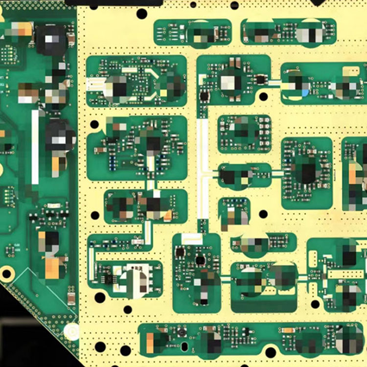
Heavy copper PCB forms a high-depth copper layer network during the electroplating deposition process through structurally enhanced conductor layer construction technology. The geometric expansion of its conductive cross section significantly optimizes the physical bottleneck of current transmission. The current-carrying effect brought by the mass accumulation of the copper layer simultaneously improves the time gradient relationship between Joule heat generation and dissipation, making the heat flux density distribution tend to be balanced.

The conductor layer of conventional circuit boards is constrained by the basic manufacturing paradigm. When maintaining the same current carrying capacity, it is necessary to use the space occupation expansion strategy, which causes the availability of the wiring channel to be compromised. The thermal expansion difference between the substrate and the copper layer presents nonlinear response characteristics in the thick copper system, and the interlayer displacement accumulation effect needs to be controlled by rheological regulation of the bonding interface. The engineering improvement of mechanical interlocking strength directly affects the interface slip suppression ability of the composite structure under dynamic load. This performance index constitutes the key threshold parameter for the reliability of the multi-layer circuit system.
During the manufacturing process, the etching process of heavy copper PCB faces the contradiction between side etching control and line width accuracy, and it is necessary to adjust the etching solution concentration gradient and spray pressure parameters. The current density distribution uniformity in the copper plating stage is required to be higher to prevent the proliferation of tumors on the edge of the line caused by local excessive thickness. In contrast, the etching window of ordinary circuit boards is wider and the process tolerance is relatively high.
In terms of heat dissipation design, heavy copper PCBs can achieve three-dimensional heat flow guidance through embedded copper blocks or local thick copper areas, while ordinary circuit boards mostly rely on external heat sinks for passive heat dissipation. In terms of long-term reliability, the thick copper structure of heavy copper PCBs significantly improves the ability to suppress electromigration, delaying the risk of short circuits caused by the growth of metal whiskers.
