

High Density Interconnect (HDI) printed circuit boards represent a refined class of circuit board technology designed to meet the increasing demand for compact, lightweight, and high-performance electronic devices. HDI PCB structures incorporate microvias, fine traces, reduced pitch components, and multilayer stacking to deliver greater wiring density within smaller footprints. The purpose of this article is to explore what HDI PCBs are, why they are essential for today’s electronics, how they function in different applications, and what trends will shape their future development.
HDI PCBs solve the challenge of dense routing in advanced electronics such as smartphones, wearable devices, automotive control systems, medical miniaturized modules, 5G communication hardware, industrial automation equipment, and aerospace electronics. Their enhanced electrical performance and space-saving structure make them ideal for devices requiring fast signal transmission, improved reliability, and reduced electromagnetic interference.
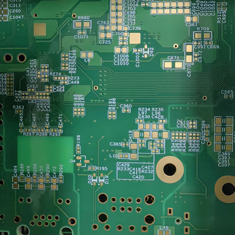
A professional understanding of HDI PCB characteristics can be greatly strengthened by reviewing their technical specifications. Below is a parameter list that outlines the key structural and performance attributes commonly requested in the industry.
| Parameter | Specification |
|---|---|
| Layer Count | 4–20 layers or custom configurations |
| Via Structure | Microvias, buried vias, blind vias, stacked or staggered |
| Minimum Line Width / Space | As low as 50/50 μm depending on capability |
| Dielectric Thickness | 40–100 μm based on design |
| Copper Thickness | 0.5–2 oz depending on current requirements |
| Material Options | FR4 High-Tg, Polyimide, BT resin, Halogen-free materials |
| Aspect Ratio | Typically 0.75:1 for microvias |
| Solder Mask | LPI, matte, glossy, multiple color options |
| Surface Finish | ENIG, ENEPIG, immersion silver, immersion tin, OSP |
| Impedance Control | ±10% tolerance or tighter |
| Thermal Conductivity | 0.3 W/m·K to 2.0 W/m·K depending on material |
| Reliability Testing | Thermal cycling, IST, CAF resistance, microsection analysis |
These parameters help define the mechanical, electrical, and thermal performance of an HDI PCB, ensuring compatibility with high-density semiconductor packages such as BGA, CSP, LGA, and advanced SoC modules.
The adoption of HDI PCB technology has increased dramatically because of the unique performance advantages it offers in modern electronic engineering. Understanding why HDI PCBs outperform conventional PCBs requires examining their structural benefits, electrical behavior, and usage flexibility.
HDI PCBs support advanced packaging technologies, enabling more components to be integrated into smaller areas. This is essential for consumer electronics and compact industrial modules.
Shorter signal paths reduce propagation delay, improve signal integrity, and support high-speed, high-frequency circuits such as RF modules, 5G antennas, and high-bandwidth memory interfaces.
The compact structure and optimized copper distribution enhance heat dissipation efficiency. This is especially important in devices with continuous or heavy data processing.
Consistent layer stacking and controlled impedance help minimize crosstalk, making HDI an ideal solution for sensitive communication, navigation, and medical electronics.
Despite thin dielectric layers and fine traces, HDI PCBs offer enhanced mechanical integrity, making them suitable for wearables, automotive environments, and industrial vibration-resistant devices.
Structures such as 1+N+1, 2+N+2, or even 3+N+3 enable complex routing needed for processors and memory systems that require layered connectivity.
These performance characteristics highlight why HDI PCBs are widely used in IoT devices, communication hardware, and advanced automotive electronics. The benefits are not limited to size reduction; they extend to signal fidelity, durability, and system-level reliability.
To understand how HDI PCBs support sophisticated modern systems, it is crucial to explore their structural functioning, manufacturing processes, and practical engineering design concepts.
Microvias are extremely small laser-drilled holes connecting adjacent layers. Their small diameter reduces space requirements, enabling denser routing and better current flow. Stacked microvias allow high-current or high-speed connections to pass through multiple layers without affecting signal quality.
HDI PCBs are often produced through a multilayer buildup process. Layer groups are laminated in multiple stages, allowing blind and buried vias to be placed precisely. This provides effective routing solutions for high-pin-count ICs.
The controlled impedance design and precise dielectric thickness make HDI PCBs ideal for high-speed differential signals such as USB 3.2, HDMI 2.1, PCIe, and RF circuits.
Thermal vias, heat-spreading copper coins, and metal base layers are frequently added to enhance thermal conductivity and ensure stable operation in high-power modules.
Advanced imaging and etching processes allow line widths as small as 50 μm, enabling precise routing under BGA components and saving board space for additional features.
CAF-resistant materials and strict thermal cycling tests ensure that HDI PCBs maintain stability in harsh environments such as automotive ECUs, aerospace control modules, and industrial power systems.
By integrating these manufacturing and design techniques, HDI PCBs serve as functional cores for products requiring miniaturization without compromising electrical, thermal, or mechanical performance.
As electronic products continually evolve, HDI PCB technology is also transforming to meet higher performance demands. Several future trends highlight the direction of HDI PCB development.
HDI PCBs are essential for 5G signal modules because they require tight impedance control and ultra-low loss materials. Next-generation 6G communication will demand even more advanced HDI structures.
Future HDI boards are expected to embed passive components or even active chips directly within the board layers, reducing overall device thickness and improving signal paths.
Wearables, medical implants, and foldable devices are pushing the demand for semi-flexible HDI boards combining rigidity with flexible bending.
Low-Df, low-Dk materials will become standard to support ultra-high-speed digital interfaces and mmWave communication applications.
Sustainability requirements will continue to drive the adoption of halogen-free resins, lead-free surface finishes, and greener production technologies.
While not discussed directly in the article content, the market demand for compact, efficient, and processing-dense devices indirectly boosts the adoption of HDI PCB structures.
These trends indicate that HDI PCBs will maintain an essential position in advanced product design across various industries, from consumer electronics to industrial and automotive systems.
Q: What is the main difference between an HDI PCB and a standard multilayer PCB?
A: An HDI PCB incorporates microvias, finer lines, and high-density component placement, enabling compact structures and superior electrical performance. Standard PCBs use larger vias and have lower routing density, making them less suitable for miniaturized devices or high-speed circuits.
Q: How does the HDI PCB structure improve signal integrity in high-frequency applications?
A: The shorter signal paths, tightly controlled impedance, reduced via stubs, and optimized layer stackups minimize loss, reflection, and crosstalk. These features create a stable environment for high-frequency signals and ensure consistent performance in communication and computing devices.
HDI PCB technology continues to play a vital role in shaping the future of advanced electronic design. With its ability to provide compact structures, support high-density components, deliver enhanced electrical performance, and ensure reliable operation, it has become fundamental in industries ranging from communication and computing to automotive and medical applications. As demand increases for smaller, faster, and more powerful electronics, HDI PCBs will continue evolving through advanced materials, embedded components, and innovative manufacturing techniques.
For high-reliability and high-density PCB solutions, the expertise and production capabilities of Hayner ensure that product performance aligns with the evolving needs of global markets.
For professional HDI PCB support and customization, contact us today.


