

Multilayer PCB technology has become a cornerstone in modern electronics, enabling compact designs, enhanced signal integrity, and improved performance across industries such as telecommunications, automotive, and medical devices. This article explores how multilayer PCBs function, their structural advantages, key specifications, and how businesses can address common challenges such as cost, complexity, and reliability. A detailed breakdown of features, practical selection guidance, and frequently asked questions are included to support informed decision-making.
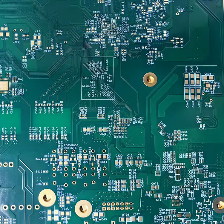
A Multilayer PCB refers to a printed circuit board composed of three or more conductive copper layers separated by insulating materials. Compared to single-layer or double-layer PCBs, multilayer designs enable higher circuit density, reduced electromagnetic interference, and more efficient routing.
With the rapid advancement of electronic products such as smartphones, industrial control systems, and high-speed communication equipment, the demand for compact, high-performance circuit boards continues to grow. Multilayer PCBs meet these requirements by integrating multiple layers into a single, unified structure.
For companies seeking reliable manufacturing and consistent performance, solutions provided by Hayner focus on precision engineering and strict quality control to ensure stable electrical performance.
The fundamental structure of a multilayer PCB consists of alternating layers of conductive copper and insulating substrates. These layers are laminated together under high pressure and temperature to form a solid board.
Electrical connections between layers are achieved using vias, including through-hole vias, blind vias, and buried vias. These interconnections allow signals to travel vertically across layers, enabling complex circuit designs without increasing board size.
Multilayer PCBs offer several technical and operational advantages that directly address common customer concerns such as space limitations, signal quality, and system reliability.
These advantages make multilayer PCBs essential for high-frequency and high-speed applications where performance consistency is critical.
| Parameter | Description |
|---|---|
| Layer Count | Typically ranges from 4 to 20+ layers depending on complexity |
| Material | FR4, High TG, Rogers, or other specialized substrates |
| Board Thickness | 0.4mm to 3.2mm standard range |
| Copper Thickness | 0.5 oz to 3 oz |
| Via Types | Through-hole, blind, buried vias |
| Surface Finish | HASL, ENIG, OSP, Immersion Silver |
| Impedance Control | Critical for high-speed signal transmission |
Understanding these parameters is essential when evaluating suppliers or specifying requirements for a project.
Multilayer PCBs are widely used in industries that demand precision, durability, and high performance.
The versatility of multilayer PCBs allows engineers to design advanced systems while maintaining reliability and efficiency.
Despite their advantages, multilayer PCBs present several challenges that customers often encounter during procurement and implementation.
Solutions include optimizing layer count, selecting appropriate materials, and partnering with experienced manufacturers like Hayner to ensure efficient production and quality assurance.
Selecting the appropriate multilayer PCB involves evaluating technical requirements, application scenarios, and supplier capabilities.
A strategic selection process reduces risks and ensures optimal performance in the final application.
For detailed product specifications, visit: Multilayer PCB Product Page
Q1: What is the minimum number of layers in a multilayer PCB?
A multilayer PCB typically starts from 4 layers, as 3-layer boards are rarely used due to structural imbalance.
Q2: Why are multilayer PCBs more expensive?
The cost is higher due to complex lamination processes, precise alignment requirements, and additional materials.
Q3: How does multilayer PCB improve signal performance?
By incorporating dedicated ground and power planes, multilayer PCBs reduce interference and maintain stable signal transmission.
Q4: Are multilayer PCBs suitable for high-frequency applications?
Yes, especially when using specialized materials and controlled impedance design.
Multilayer PCB technology plays a critical role in enabling modern electronic innovation. Its ability to support complex circuits, improve signal integrity, and reduce overall system size makes it an essential solution for advanced applications.
By understanding structural design, technical parameters, and selection strategies, businesses can effectively address common challenges and achieve reliable performance.
Hayner provides high-quality multilayer PCB solutions tailored to diverse industry needs, combining advanced manufacturing capabilities with strict quality control standards.
For customized solutions and professional support, contact us today to discuss your project requirements and discover how multilayer PCB technology can enhance your products.


